
2021.09.14
MOS tube switch tube loss calculation method formula detailed explanation
MOSFET switching loss
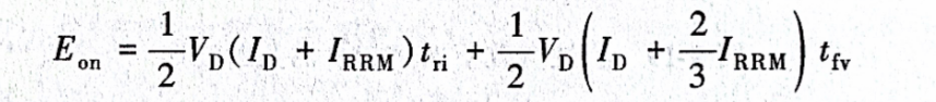
The maximum switching frequency that a power MOSFET can achieve depends on the switching loss. The energy loss of each pulse period can be estimated just like other devices. It can be calculated by integrating the product of V(t) and i(t) during the turn-on and turn-off process. During the opening period, it can be estimated as
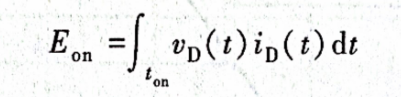
In actual situations, the energy loss of each pulse is determined by the waveform diagram. Modern oscilloscopes can calculate the product of current and voltage and integrate within a selected time for estimation
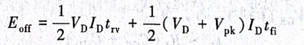
It is assumed that at the moment of Tfv, the maximum reverse current IRRM caused by the diode decays linearly. For the turn-off process, the energy loss can be estimated as
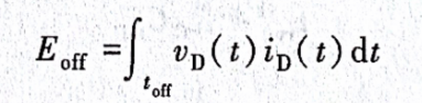
It can be seen that its value is approximately
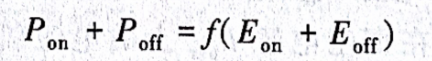
The total switching loss is determined by the following formula:
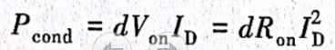
The conduction loss and blocking loss must be added to the switching loss. For the power MOSFET, the leakage current in the blocking state is about a few microamperes, so the blocking loss can be ignored. The conduction loss is not negligible.
The duty cycle d is defined as the ratio of the MOSFET on to the interval of the entire switching cycle. The conduction loss can be estimated according to the following formula:
The total loss can be obtained by
These losses can only be transferred out of the shell and tube by heat flow. The maximum allowable loss is determined by the heat dissipation conditions, the tolerable temperature difference and thermal resistance.
For the example MOSFET IXYS IXFH 67 N10, the maximum switching frequency can be estimated from the thermal resistance value in the data sheet to 300kHz. Obviously, as a unipolar device, MOSFET is the fastest Si semiconductor switching device available.
The potential switching frequency depends on the thermal parameters on the one hand, but also on other devices in the circuit, so the entire circuit must be optimized. From equation (9-34) and equation (9-36), it can be seen that the switching loss is determined by the switching time. A smaller gate resistance Rc can reduce the switching time, which can reduce the switching loss. On the other hand, the steepness of the slope is also limited in practice:
1) The limitation of motor windings, it can not resist too high dv/dt.
2) It is also limited by the freewheeling diode which is indispensable in the inductive circuit. Improper selection of freewheeling diode
In other words, increasing di/dt will lead to rapid switching characteristics, voltage spikes and oscillations.

Introduction to MOSFET production process
2021.09.09
From the beginning of production to the completion of the manufacturing of semiconductor products, there are mainly two processing processes, which are called front-end production and back-end production.

Key Points of the Design and Layout of Semiconductor Wafer Shop
2021.09.10
During the production process of semiconductor device wafers, it is easy to be affected by foreign objects, dust particles, metal ions and other foreign objects to destroy the surface structure.

What is wafer testing? How to perform wafer test?
2021.09.10
Wafer testing is to test each die on the wafer, attach a probe made of gold wire to the inspection head to make a probe (probe) as thin as a hair, and contact the pad on the die to test its electrical Characteristics
Technical advantages
Product Center
Industry Application
News Center