
Semiconductor companies continue to face complex integration challenges because consumers want their electronic products to be smaller, faster, and perform better, and integrate more functions into a single device. Semiconductor packaging has a major impact on solving these challenges. The current and future requirements for improving system performance, increasing functions, reducing power consumption, and shrinking form factors require an advanced packaging method called system integration.
System integration can combine multiple integrated circuits (ICs) and components into a single system or modular subsystem to achieve higher performance, functionality, and processing speed, while greatly reducing the space requirements inside electronic devices. .
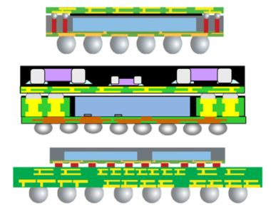
The advantages of FZWELEC in SiP packaging are reflected in three advanced technologies: double-sided molding technology, EMI electromagnetic shielding technology, and laser assisted bonding (LAB) technology.
1. Double-sided molding effectively reduces the package size, shortens the connection of multiple bare chips and passive devices, reduces resistance, and improves the electrical performance of the system.
2. For EMI shielding, JCET uses back metallization technology to effectively improve thermal conductivity and EMI shielding.
3. JCET uses laser-assisted bonding to overcome traditional reflow bonding problems, such as CTE mismatch, high warpage, high thermal mechanical stress and other reliability problems.
Solution
eWLB-PoP & 2.5D SiP
Technical advantages
Product Center
Industry Application
News Center