2021.09.13
Introduction to the structure and function of discrete devices
Discrete devices refer to electronic devices that have separate functions and cannot be separated. They can be divided into semiconductor diodes, triodes, bridge rectifiers, optoelectronic devices, etc. according to the chip structure and function. Semiconductor discrete devices are mainly composed of a chip, a lead/frame, and a plastic enclosure. The chip determines the device function, such as rectification, voltage stabilization, switching, protection, etc. The lead/frame realizes the connection between the chip and the external circuit and the export of heat, plastic packaging The shell provides protection for the chip and internal structure to ensure the stable realization of its functions, and is highly related to core performance such as heat dissipation.
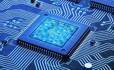
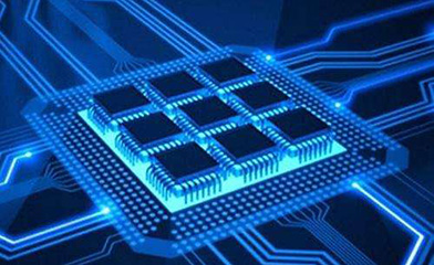
Discrete device chips are different from integrated circuit chips commonly understood in the semiconductor industry. The basic unit for the realization of the function of a semiconductor circuit is a PN junction composed of semiconductor materials. The PN junction and the pattern formed by it are engraved on a small piece of silicon in a certain manner to form a semiconductor chip. Among them, the discrete device (diode, triode, etc.) chip refers to a chip in which only one or a small amount of PN junction is formed on a silicon chip through doping, diffusion and other processes. The chip has a simple structure and relatively simple function, mainly to achieve Established circuit functions such as rectification, voltage stabilization, switching, and amplification. The integrated circuit chip uses a special semiconductor process to engrave thousands of PN junctions, capacitors, resistors, wires and other patterns with specific functions on a small piece of silicon to form a chip. Therefore, the structure of the integrated circuit chip is very complicated. Complicated functions such as processing and conversion of digital signals and analog signals can be realized.
Although the integration of the chip brings the advantages of small size, light weight, and high reliability, but for some specific functions that are difficult to integrate, such as high-speed switching, voltage stabilization protection, transient suppression, and performance requirements such as high current, high voltage, and low power , And considering the circuit structure, integration difficulty, cost, stability and other aspects, a large number of discrete devices are still needed to complete. Therefore, the use of discrete devices and integrated circuits has become the norm in the semiconductor industry.
Product Classification of Discrete Devices
半导体分立器件按照芯片结构和功能可区分为二极管、三极管,以及由其通过一定方式连接形成的器件(如整流桥)。半导体产业起步于上世纪50年代,在发展历程中,半导体二极管、双极型晶体管(BJT)、场效应晶体管(Power-MOSFET)、绝缘栅双极型晶体管(IGBT)等先后出现,一般将双极型晶体管、场效应晶体管和绝缘栅双极型晶体管统称为三极管。
随着半导体产业的逐步发展,对芯片供电mA级别的电流需求、产品良率及成本制约下小功率器件无法集成、下游产品对半导体分立器件体积要求越来越苛刻等问题逐步凸显,无论是二极管还是三极管,在制造工艺上均面临突破上述发展瓶颈的需要。为解决上述问题,体积较小且通过电流较小的“小信号器件”概念开始被台湾分立器件厂商单独列出,并形成了一系列专业的工艺方法,可以用于各类二极管、三极管的生产。
随着小信号器件概念的出现,半导体分立器件在按照芯片结构、功能划分维度之外,又可按照功率、电流指标划分为小信号器件及功率器件两大类。世界半导体贸易统计协会(WSTS)将小信号器件定义为耗散功率小于1W(或者额定电流小于1A)的分立器件,而耗散功率不小于1W(或者额定电流不小于1A)的分立器件则归类为功率器件。
小信号器件与功率器件在生产工艺和产品应用方面存在显著差异。小信号器件芯片尺寸和封装尺寸均较小,对生产作业控制精度要求较高,对机械化自动化要求很高,并由于产品组件比较脆弱,需要在生产过程中给予很好的保护,同时其电性参数值均比较小,因此要求测试系统能够快速分辨出微小的电量变化,具备较高的测试精度。而功率器件芯片尺寸和封装尺寸都比较大,要求芯片与框架接触良好、封装体有较好的散热能力、封装应力尽可能小、测试过程中能够提供大电流高电压、并进行不同测试参数条件下自动比对筛选。由于前述差异,在半导体产业逐步专业化发展的过程中,器件在生产工艺及产品应用方面的差异程度超出了其在芯片结构及功能方面本身的差异,小信号器件、功率器件的概念逐步被普遍接受。
The classification of discrete devices based on power and current is a common classification method in the industry. The latest "White Paper on Power Semiconductor Discrete Device Industry and Standardization (2019 Edition)" released by the China Electronics Standardization Institute in November 2019 divides discrete devices into small signal devices and power devices; the World Semiconductor Trade Statistics Association (WSTS) in its products The classification manual also adopts the classification of small signal devices and power devices according to the power standard; Gartner, the world's most authoritative IT research and consulting company, divides discrete devices into small signal devices, power devices, and radio frequency devices; Toshiba, a well-known company in the industry , Rohm, Anshi, Vishay, China Resources Micro, Yangjie Technology, etc. have adopted the aforementioned classification methods in their product manuals.

Introduction to MOSFET production process
2021.09.09
From the beginning of production to the completion of the manufacturing of semiconductor products, there are mainly two processing processes, which are called front-end production and back-end production.
Key Points of the Design and Layout of Semiconductor Wafer Shop
2021.09.10
During the production process of semiconductor device wafers, it is easy to be affected by foreign objects, dust particles, metal ions and other foreign objects to destroy the surface structure.
What is wafer testing? How to perform wafer test?
2021.09.10
Wafer testing is to test each die on the wafer, attach a probe made of gold wire to the inspection head to make a probe (probe) as thin as a hair, and contact the pad on the die to test its electrical Characteristics
Technical advantages
Product Center
Industry Application
News Center